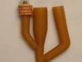

圖示:a.全金屬邏輯非門電路。由兩個50nm線寬的Invar點接觸結(jié)構(gòu)(CF,,ED)和兩個400納米線寬的Invar金屬線(CE,,F(xiàn)D)構(gòu)成。b.非門電路隨時間變化的輸入與輸出特性,。
近日,,中科院物理所微加工實驗室顧長志研究員領(lǐng)導(dǎo)的研究組與表面物理國家重點實驗室夏鈳研究員領(lǐng)導(dǎo)的研究組合作,設(shè)計并制作出全金屬納米結(jié)構(gòu)的邏輯電路,。相關(guān)工作發(fā)表在2月3日出版的《自然—納米技術(shù)》(Nature Nanotechnology)2008年第2期上,。
磁性材料可以作為信息存儲和信息處理的基本單元。而納米磁性材料器件所表現(xiàn)的優(yōu)異特性使我們可以得到更快的信息處理速度和更高的信息存儲密度,,并由此導(dǎo)致自旋電子學(xué)的加速發(fā)展,。自旋電子學(xué)的目的就是在以電荷為信息載體的基礎(chǔ)上增加自旋作為信息的載體,這對整個信息產(chǎn)業(yè)的發(fā)展具有深遠的意義,。目前,,已經(jīng)出現(xiàn)的自旋邏輯器件有電驅(qū)動、磁檢測,,磁驅(qū)動,、電檢測,或者磁驅(qū)動,、光檢測,,但是它們都有一定的局限性。而現(xiàn)今的信息技術(shù)都是建立在利用電信號的基礎(chǔ)上,,所以實現(xiàn)電驅(qū)動和電檢測的自旋邏輯器件對自旋電子學(xué)在信息技術(shù)領(lǐng)域的應(yīng)用具有重要意義,。
自旋極化電流與天然存在的磁疇壁間的角動量交換打開了磁與電之間聯(lián)系的新通道。不需要外加磁場,,僅用電流來操縱材料的磁化狀態(tài),,克服了磁場難以屏蔽的困難,為自旋邏輯器件高度集成和信號高可靠性處理提供了可能,。中國科學(xué)院物理研究所微加工實驗室顧長志研究員領(lǐng)導(dǎo)的小組與表面物理國家重點實驗室夏鈳研究員領(lǐng)導(dǎo)的課題組合作,,通過鐵磁金屬因瓦合金納米點接觸結(jié)構(gòu)的設(shè)計和納米加工,在認(rèn)真研究電流驅(qū)動疇壁與納米點接觸電阻關(guān)系的基礎(chǔ)上,,設(shè)計并制作出基于疇壁運動的邏輯“非門”電路,。其工作的基本原理是:鐵磁金屬納米點接觸結(jié)構(gòu)能夠在點接觸位置釘扎住一個磁疇壁,并在自旋極化電流驅(qū)動下運動,,使點接觸電阻在高阻與低阻態(tài)間來回轉(zhuǎn)換,,配合一個具有固定電阻的金屬納米線作為參考電阻與之相比較,將點接觸結(jié)構(gòu)和金屬納米線串聯(lián)之后聯(lián)入電源兩端,,點接觸和納米線之間的連接點的電勢會因為點接觸電阻的改變而發(fā)生變化,,電勢的高低可以定義為邏輯信號,,代表二進制的“0”和“1”。
這種邏輯電路在室溫條件下直接用電信號驅(qū)動,,并且使用電信號探測,,具有集成度高、成本低,、兼容性好和低功耗的特點,,能夠在磁性材料的居里溫度以下正常工作(600℃),并與現(xiàn)今的CMOS平面工藝完全兼容,。由于電路以全金屬結(jié)構(gòu)實現(xiàn),,能夠獲得比現(xiàn)今的半導(dǎo)體電路更高的載流子密度和更細(xì)的線寬,為新型高密度納米電路的研制奠定了基礎(chǔ),。
該工作得到國家自然科學(xué)基金委,、中國科學(xué)院和科技部的資助。(來源:中科院物理研究所)
(《自然—納米技術(shù)》(Nature Nanotechnology),,3, 97 - 100 (2008) doi:10.1038/nnano.2008.1,,Peng Xu, Ke Xia, Changzhi Gu, Ling Tang, Haifang Yang & Junjie Li)
生物谷推薦原始出處:
Nature Nanotechnology 3, 97 - 100 (2008)
Published online: 3 February 2008 | doi:10.1038/nnano.2008.1
Subject Categories: Electronic properties and devices | Nanomagnetism and spintronics
An all-metallic logic gate based on current-driven domain wall motion
Peng Xu1, Ke Xia1, Changzhi Gu1, Ling Tang1, Haifang Yang1 & Junjie Li1
Abstract
The walls of magnetic domains can become trapped in a ferromagnetic metallic point contact when the thickness of the film and the width of the contact are less than their critical values1. The discovery that domain walls can be moved from such constrictions by a sufficiently large current has attracted considerable attention from researchers working on both fundamental research and potential applications2, 3, 4, 5, 6, 7, 8, 9, 10, 11, 12. Here we show that Invar nanocontacts fabricated on silica substrates exhibit a sharp drop in resistance with increasing bias voltage at room temperature in the absence of an applied magnetic field. Moreover, when two nanocontacts are combined in an all-metallic comparison circuit, it is possible to perform logical NOT operations. The use of electrical currents rather than applied magnetic fields to control the domain walls also reduces energy consumption and the risk of crosstalk in devices13, 14.
Beijing National Laboratory for Condensed Matter Physics, Institute of Physics, Chinese Academy of Sciences, Beijing 100080, China
Correspondence to: Ke Xia1Changzhi Gu1 e-mail: [email protected]